Atomera Incorporated (ATOM)
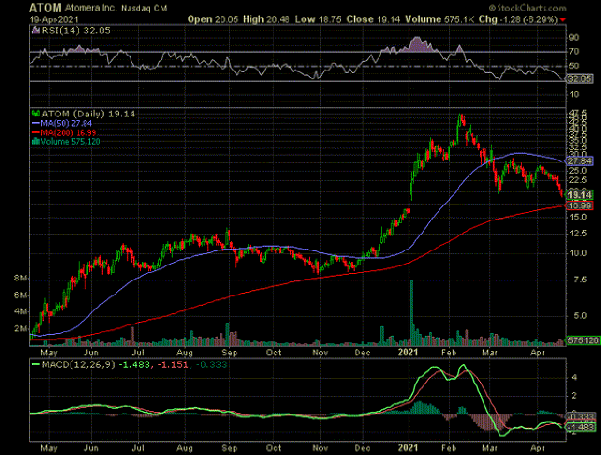
Atomera Incorporated (ATOM) is a semiconductor materials and intellectual property licensing company focused on deploying its proprietary technology into the $450+ billion semiconductor industry. Atomera has developed Mears Silicon Technology, which increases performance and power efficiency in semiconductor transistors. Mears Silicon Technology is a thin film used to enhance semiconductors results in higher performance, lower power, and lower costs. Mears Silicon Technology can be implemented using equipment already deployed in semiconductor manufacturing facilities and is complementary to other nano-scaling technologies already in the semiconductor industry roadmap. Mears Silicon Technology enhances transistors to deliver significantly better performance in today’s electronics by using a material that enhances transistors to improve performance. Large semiconductor providers license the technology in order to incorporate Mears Silicon Technology into their silicon wafer manufacturing process. Some of the benefits of Mears Silicon Technology include a longer battery life for mobile phones, making smaller Internet of Things (IoT) devices even smaller, and making web servers even more powerful. Just two and a half short months ago ATOM was traded up to $47.13. A look at the chart shows shares of ATOM deep in oversold territory.
Atomera was founded in 2001 by Robert Mears with a vision to develop a platform of materials technologies for use across multiple industries. In response to the slowdown in the advancement of Moore’s Law, Atomera used atomic level material science to develop Mears Silicon Technology which provides multiple benefits to industry participants. Moore’s Law was an observation made by Intel co-founder Gordon Moore in 1965. Mr. Moore found the number of transistors on a chip doubles every year, but industry observers have suggested that the trend, which has lasted decades, may soon end. Atomera says that MST extends Moore’s Law by allowing semiconductor manufacturers to improve power and efficiency within the same process node. For semiconductor designers Mears Silicon Technology improves performance and power efficiency while potentially reducing cost. For semiconductor fabs, the technology allows them to extend the life of their expensive manufacturing facilities by providing a new, unexpected suite of material improvements within existing process nodes. After several years of research to perfect the technology, Atomera is now engaged with leading semiconductor companies to integrate Mears Silicon Technology into their manufacturing flow.
Atomera’s management believes that the Company’s success is dependent upon the adoption of its MST technology through the Distribution stage by at least one IDM, foundry, or fabless semiconductor manufacturer.
Business Model
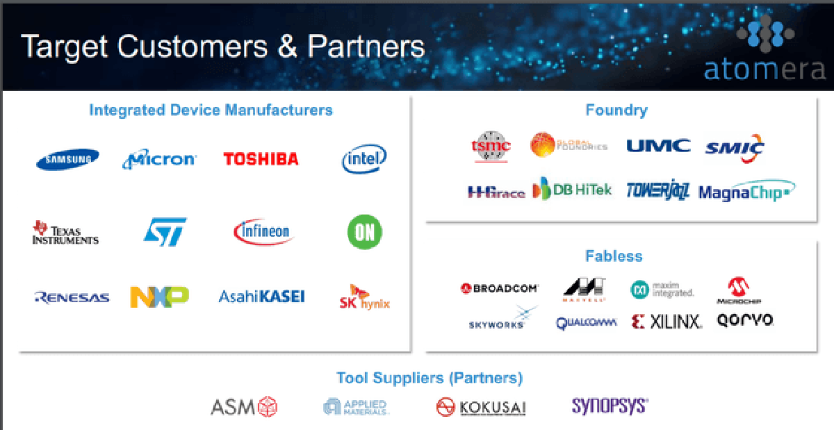
Atomera does not intend to design or manufacture integrated circuits directly. Instead, the Company develops and license technologies and processes that its management believes offers the designers and manufacturers of integrated circuits a low-cost solution to the industry’s need for greater performance and lower power consumption. Atomera’s customers and partners include:
- Foundries, which manufacture integrated circuits on behalf of fabless manufacturers.
- Integrated device manufacturers, or IDMs, which are the fully integrated designers and manufacturers of integrated circuits.
- Fabless semiconductor manufacturers, which are designers of integrated circuits that outsource the manufacture of their chips to foundries.
- Original equipment manufacturers, or OEMs, which manufacture the epitaxial, or EPI, deposition machines used to deposit semiconductor layers, such as the MST film onto the base silicon wafer.
- Electronic design automation companies, which make tools used throughout the industry to simulate the performance of semiconductor products using different materials, design structures and process technologies.
Atomera’s revenue model is based on licensing arrangements whereby its customers initially pay the Company a fee for an integration license that provides them the right to use MST technology in the manufacture of silicon wafers for internal testing and sampling. Atomera’s management plans for each integration license agreement to be the first of a three-stage licensing process with the customer, with the first integration stage to be followed by one or more agreements granting them manufacturing and distribution licenses. These are referred to as the second and third stages, respectively. Atomera expects that agreements granting manufacturing and distribution licenses will provide for substantially larger upfront license fee payments than the integration licenses and distribution agreements will require licensees to make royalty payments to us based on the number and sales price of MST-enabled products they sell to their customers. Starting in 2019, Atomera began to develop deeper relationships with several large potential customers who were evaluating MST across multiple manufacturing processes and product lines. The Company has begun proposing an engagement format called a joint development agreement, or JDA, to certain customers. Atomera expects that JDAs will be customized to a particular customer’s goals but that generally they will include development, manufacturing and licensing components.
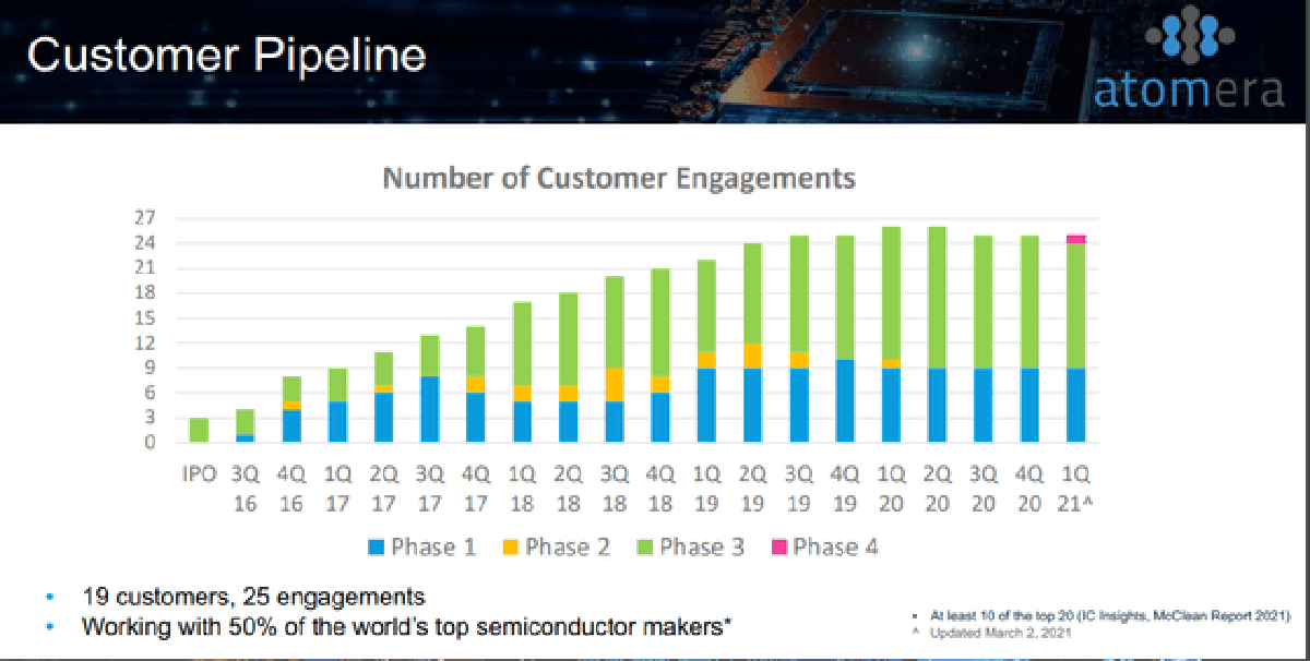
Atomera’s management believes that the Company’s success is dependent upon the adoption of its MST technology through the Distribution stage by at least one IDM, foundry, or fabless semiconductor manufacturer. In January 2021 Atomera entered into a JDA with a leading semiconductor provider for integration of its MST technology into their manufacturing process. The JDA includes the grant of an upfront, paid manufacturing license allowing the customer to install the recipe for Atomera’s MST film into a tool in their fab and to fabricate semiconductor wafers incorporating MST for use in their products, as well as development milestones that, if achieved, could result in additional revenue to Atomera. Although this JDA does not confer commercial distribution rights, Atomera’s management believes that successful execution would be a significant step toward commercialization and provide opportunities for additional license revenues and potential royalty streams from one or more of its customer’s multiple production lines. On March 2, 2021 Atomera announced it advanced its previously announced JDA customer to the fourth phase of its customer engagement process, indicating that Atomera has delivered its MST IP transfer package in accordance with JDA contract. With this advancement, the JDA customer became the first Atomera customer to enter the fourth phase of the six-phase engagement process, which culminates in commercialization of MST-enabled wafers. Atomera currently has 25 engagements in its customer pipeline, consisting of nine in phase one, 15 in phase three, and one in phase four. In its corporate deck, Atomera lists Applied Materials (AMAT) among its partners, as well as Texas Instruments Incorporated (TXN), Micron Technology, Inc. (MU), and Intel (INTC) as its target customers. Upon delivery of Atomera’s IP transfer package and issuance of its invoice, the JDA customer will move from phase three into phase four. Subject to process and subsequent product qualifications that demonstrate, in commercial scale production, the enhancements the Company believes its MST technology offers, including increased speed, reliability and energy efficiency. Atomera expects to license its MST technology to one or more of these companies.
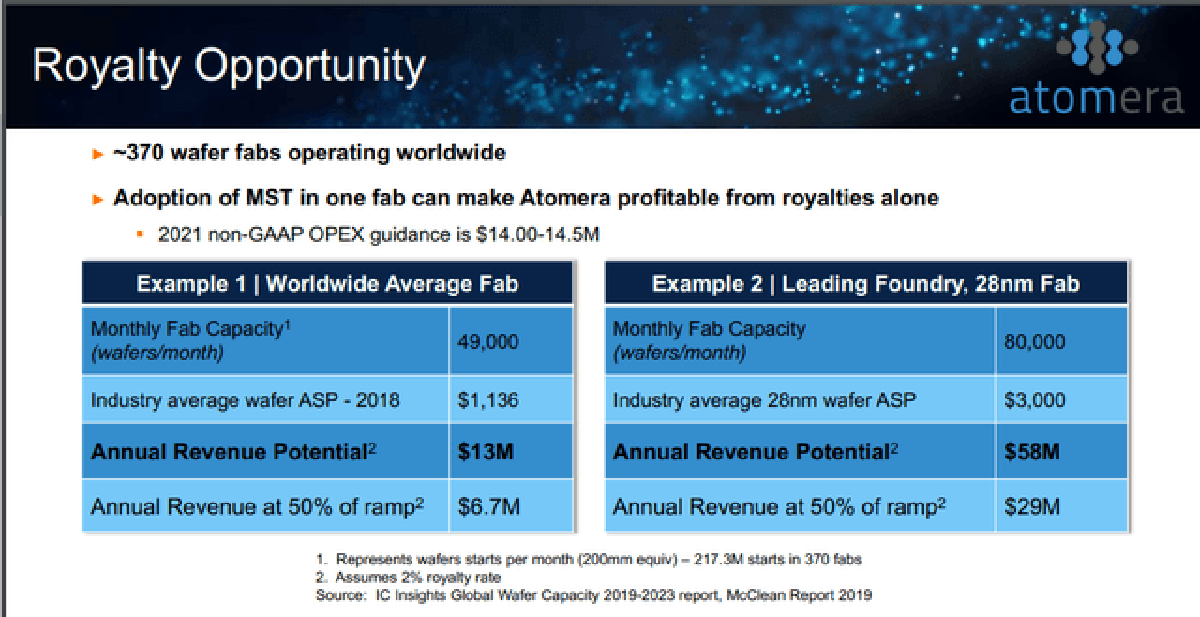
There are currently somewhere around 370 wafer fabs operating worldwide. The adoption of Mears Silicone Technology in one fab can make Atomera profitable from royalties alone. That being said, like a lot of growth companies, Atomera has a history of significant operating losses and the Company anticipates continued operating losses for at least the near term. For the years ended December 31, 2020 and 2019, Atomera incurred net losses of approximately $14.9 million and $13.3 million, respectively, and its operations have used approximately $12.1 million and $10.4 million of cash, respectively.
Atomera is also working with OEMs on process development and equipment optimization to ensure that MST can be reliably and predictably deposited using their manufacturing tools. The Company has successfully deposited MST using tools made by each of the leading epitaxial deposition equipment suppliers and management believes that if the Company is successful in its commercialization efforts, these tool OEMs will promote the incorporation of our MST technology as an option to their standard offering. By doing so, it is my opinion they will simultaneously stimulate additional sales of their capital equipment and encourage more customers to adopt MST.
Semiconductor Industry Overview
Semiconductors are included in so many everyday things that there is now a global shortage. The size of the semiconductor industry overall has grown to over $500 billion. As its overall size has increased, the equipment makers that feed it are better positioned to generate strong returns and have seen higher levels of free cash flow. Demand for chips will likely keep the overall sector growing and semiconductor manufacturers will need to continue to increase capital spending to keep pace.
Over the last few years we have seen a tremendous expansion of consumer and commercial products, especially in wireless, automotive and mobile electronic devices. The growth of the Internet and cloud computing has provided people with new ways to create, store and share information. At the same time, the increasing use of electronics in cars, buildings, appliances and other consumer products is creating a broad landscape of “smart” devices and the evolution of wearable technologies and The Internet of Things. Due to the popularity of mobile devices and other electronic products, there is increasing demand for integrated circuits and systems with greater functionality and performance, reduced size, and much less power consumption as key requirements. During 2020, the global COVID-19 pandemic accelerated trends toward remote work, cloud computing and mobile devices. These trends coincided with the rollout of 5G cellular networks and 5G-enable devices.
These developments depend, in large part, on integrated circuits, or microchips, which are sets of electronic circuits on a single chip of semiconductor material, normally silicon. It is common for a single semiconductor chip to combine many components (processor, communications, memory, custom logic, input/output) resulting in highly complex chip designs. Transistors are the building blocks of integrated circuits and the most complex semiconductor chips today contain more than a billion transistors, each of which may have features that are much less than 1/1,000th the diameter of a human hair. The most widely used transistors in semiconductor chips today are based on CMOS technology. Among its many attributes, CMOS allows for a higher density of transistors on a chip and lower power usage than non-CMOS technologies.
Better Semiconductor Performance
For years, the semiconductor industry was able to almost double the number of transistors it could pack into a single microchip about every two years, a rate of improvement commonly known as “Moore’s Law.” The semiconductor industry uses the term “node” to describe the minimum line width or geometry on a semiconductor chip, expressed in nanometers, or nm, for today’s technologies. Historically, the smaller the node, the smaller the transistors and the more closely they are packed together, producing chips that are denser and thus less costly on a per-transistor basis. Frequently, smaller nodes also correspond to an improvement in chip performance, making them the mile markers of Moore’s Law, with each node marking a new generation of chip-manufacturing technology.
Until recently, the industry succeeded at maintaining the rate of improvement predicted by Moore’s Law by scaling the key transistor parameters, such as shrinking feature sizes and reducing operating voltages, thereby allowing more transistors to be packed onto a single microchip. This trend was facilitated in large part by the development of CMOS technologies. However, a discontinuity in the rate of improvement delivered by scaling appeared when transistor technology reached feature sizes below 100 nanometers. The industry responded with advanced materials to supplement the ongoing geometry shrinks. Some of those materials advances included strained silicon, Silicon-on-Insulator and High-K/Metal Gate.
The designers and manufacturers of integrated circuits and systems — Atomera’s targeted customers — are facing intense pressure to deliver innovative products at ever shorter times-to-market, as well as at lower prices. In other words, innovation in chip and system design today often hinges on “better, sooner and cheaper.” Atomera’s management believes that the semiconductor industry has accepted that moving forward in the nano-era will require adoption of new innovations that extend the scaling formula, including those based on the use of new engineered materials, a market opportunity our MST technology seeks to address. Because shrinking geometries at the smaller nodes incurs higher capital and manufacturing costs, only a limited number of companies can afford to continue investing in those nodes. In my opinion, these constraints will cause semiconductor designers and manufacturers to turn to engineered materials, like MST, to solve this problem.
The Short Story
The short interest in the stock may be the biggest catalyst of all. Shares of Atomera have been crushed over the past 10 weeks. As of March 31, 2021 there were 2,952,916 shares short, according to NASDAQ. The average daily volume on March 31 was 429,749 shares, which means it is going to take the shorts 6.87 days to cover. It will be interesting to see the numbers for April 15, which should be out soon. On April 7, 2021 NASDAQ published a news story on Atomera’s ticker titled “What Kind Of Investors Own Most Of Atomera Incorporated (NASDAQ: ATOM)?” Shares of Atomera have traded lower every day since then. The article was written by an organization called Simply Wall Street. Simply Wall Street is not based on Wall Street. Simply Wall Street is based in Sydney Australia. Its founder is a young man named Al Bentley. According to Mr. Bentley’s LinkedIn profile he graduated from college in 2009 and he was a Graphic Graduate Engineer, a Naval Architect, and a Project Engineer. After reading the articles Simply Wall Street writes, I noticed every article is negative and bearish. Either Mr. Bentley is a very benevolent soul who wants to stop people from investing in what he thinks are bad companies, or he has an interest in seeing those companies’ shares trade lower. This, of course, is just my opinion.
In my opinion, stocks with a tight float, solid insider ownership, and strong institutional shareholders have a lot of potential to trade higher when the shorts start to cover.
Summary
Atomera has a high margin, recurring revenue financial model. The Company also has a strong balance sheet, solid technology, and a patent portfolio that has increased 17% year over year and includes 269 patents granted and pending. Atomera is gaining traction with many top industry players and growing its licensee base. This gives the Company the opportunity to ramp up its commercial license revenues.
Atomera has 23,006,449 common shares issued and outstanding as of its March 12 proxy filing. Out of the 23,006,449 common shares outstanding, institutional ownership is 26.02%, while management owns 14.4%. In my opinion, with almost 3 million shares short and a strong shareholder base, shares of ATOM could trade much higher in the near-term. The fact that the adoption of Mears Silicone Technology in one fab can make Atomera profitable from royalties alone makes Atomera a great long-term play. Atomera plans to release its first quarter 2021 financial results after the market closes on Wednesday, April 28, 2021. The company will host a live video Zoom webinar at 2:00 p.m. Pacific Time (5:00 p.m. Eastern Time) on Wednesday, April 28, 2021 to discuss the results. The live webinar can be accessed through Atomera’s investor relations website at Atomera Incorporated.

